

I came across the printed circuit board for this circuit completely by accident. It looked like an interesting and clever little design, and I had more than enough suitable parts lying around in my component drawers, including a pile of spare relays. So I decided to build one and measure what it could actually do. Here are the results.
“Baji Elektronika Amatőrbolt” is a small electronics shop in Vác, Hungary. In addition to electronic components, they sell various modules and kits of their own design. More information can be found on their website: https://bajielektronika.hu/. I had dropped in to buy some BF199 transistors when I noticed the PCBs for this relay timer in the shop’s bargain bin. The kit is no longer sold, and the remaining bare PCBs were being cleared out for €0.28 each. Since I have quite a few surplus relays that fit this board, I bought two PCBs for a bit of Saturday tinkering and assembled one using components I already had in my parts drawers.
These days, one would probably build this kind of timer around the CMOS version of the famous NE555: an ICM7555 or TLC555. These ICs operate from a supply voltage of 1.5…18 V while drawing a very low supply current of around 60–250 µA. Their timing is virtually independent of supply voltage and, depending on the quality of the timing capacitor, delays of several hours or even a full day are possible. Internally, however, the IC is relatively complex, containing roughly 40–50 MOSFETs
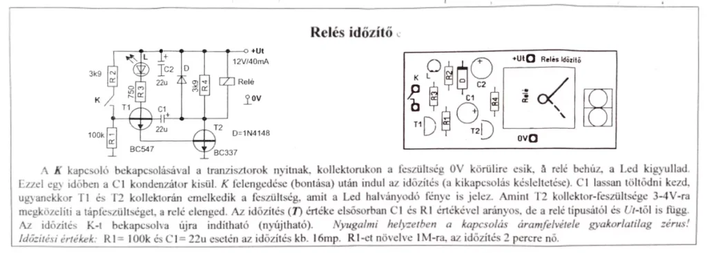
This little circuit, by contrast, contains just two bipolar transistors. One of its most interesting features is that its quiescent current consumption is practically zero: less than 0.1 µA. Looking at the schematic, the principle is surprisingly elegant. Rather than simply using the slowly changing voltage across a capacitor to switch a transistor, capacitor C1 feeds a signal back from the output at T2 to the base of T1. This allows the two-transistor circuit to operate as a genuine off-delay timer.
How Does It Work?
When switch K is closed, the relay energises and, depending on how its NO, NC and COM contacts are wired, switches the connected load either on or off. The relay remains energised and the LED stays lit for as long as K is closed. When K is opened, the LED begins to fade and, after a certain delay, the relay drops out. The timing cycle can be restarted at any time simply by closing K again. Another peculiarity of the circuit is that, when power is first applied, a timing cycle occurs even if K is left open, although this initial cycle is somewhat shorter than the nominal delay.
Let us look at the operation in more detail. When switch K is closed, the supply voltage is applied through R2 to the base of T1, a BC547. T1 turns on, and its emitter current drives T2, the higher-current BC337 transistor. T2 effectively acts as a switch: it pulls its collector close to 0 V, so almost the full supply voltage appears across the relay coil connected between +Ut and the collector. The relay therefore energises. At the same time, T1’s collector current flows through LED L and its series resistor R3, so the LED lights.
The key component determining the delay is the 22 µF capacitor C1. It is connected between the base of T1 and the collector of T2. While K is closed and T2 holds its collector close to ground potential, the previous charge on C1 is removed. This effectively resets the timer.
When K is released, the direct base drive to T1 disappears, so in principle both transistors could turn off immediately. But the voltage across a capacitor cannot change instantaneously. The relay coil and R4 begin pulling T2’s collector voltage towards the positive supply rail, and C1 couples this rising voltage to the base of T1. T1 therefore continues to receive base current and, in turn, continues to drive T2. In other words, C1 temporarily keeps the two-transistor circuit “alive”.
Meanwhile, R1 continuously pulls the base of T1 towards ground, so this condition cannot persist indefinitely. C1 gradually charges, the base current of T1 decreases, and the currents through both transistors fall. As a result, the collector voltage of T2 slowly rises towards +Ut. The voltage across the relay coil decreases correspondingly: U_relay ≈ Ut − UCE_T2.
Once the collector of T2 has risen to within approximately 3–4 V of the supply voltage, the remaining voltage across the relay coil is no longer sufficient to keep it energised, and the relay drops out. The original description specifies a 12 V supply and therefore requires a 12 V relay, but with appropriately chosen component values the circuit can also be made to operate from, for example, 5 V or 24 V.
The same process can be observed in the LED: as T1’s collector current decreases, the LED gradually becomes dimmer and eventually goes out.
There are two other neat details. The 1N4148 diode D suppresses the inductive voltage spike generated when the relay coil is switched off, thereby protecting T2. And if K is pressed again while the timer is running, T2 is driven fully on again and C1 is discharged once more. The timing cycle can therefore be restarted or extended at any time.
The most elegant feature of the circuit is its quiescent state. Once the timing cycle has ended, both transistors are off, the relay and LED are off, and K is open. There is no branch that continuously conducts between +12 V and ground. Ideally, the current consumption would therefore be exactly zero. In reality, only the leakage currents of the transistors, diode and electrolytic capacitor remain, and these are all extremely small. This explains the exceptionally low standby current of the Baji timer.
How Long Is the Delay?
The timing interval cannot be described simply by the usual T = k·R·C relationship. It is determined primarily by R1 and C1, but it also depends on the supply voltage, the characteristics of the transistors and, especially, the relay’s dropout voltage.
According to the original description, with R1 = 100 kΩ and C1 = 22 µF, the delay is approximately 16 seconds. Increasing R1 to 1 MΩ extends the delay to about 2 minutes.
One characteristic of the circuit is that it is not particularly sensitive to the exact component values. I used whatever suitable components I happened to have in my drawers, so the version I built differs somewhat from the original specification. In my circuit, R2 and R4 are both 6.2 kΩ, R1 is 1 MΩ and R3 is 820 Ω. The most important difference is that C1 and C2 are not 22 µF but approximately twice as large, at 47 µF.
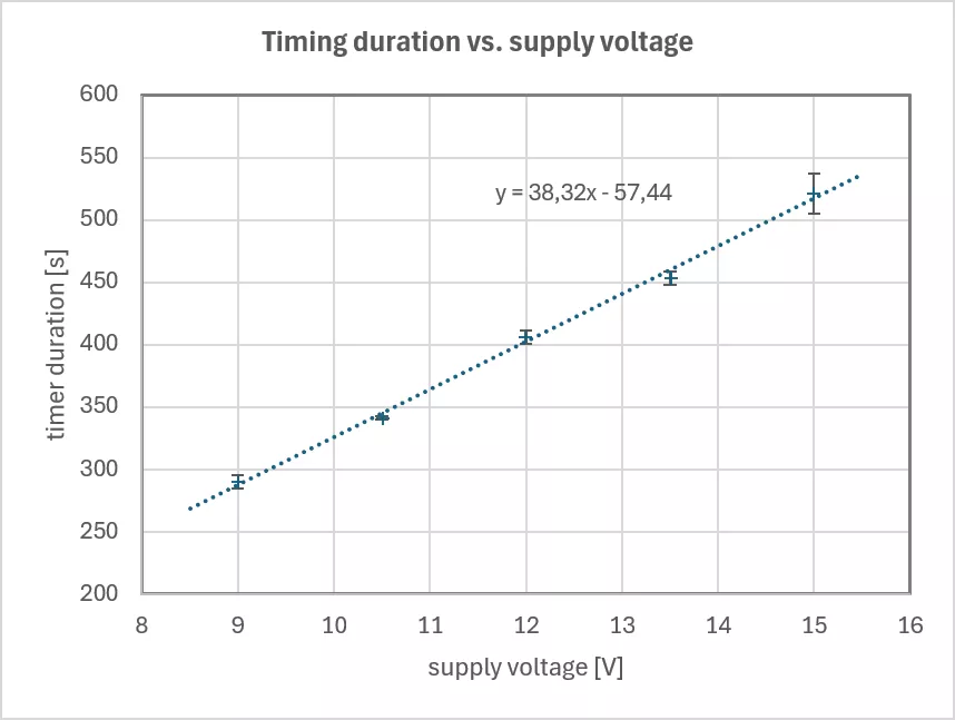
I measured the delay of the completed board by counting 1 Hz pulses passed through the relay contacts. Measurements were made at five different supply voltages between 9.0 V and 15.0 V, with five measurements at each voltage. All measurements were made from a “warm start”: after allowing the initial power-on cycle to complete and excluding it from the data, I started each of the five measurements by holding switch K closed for 10 seconds.
The results are shown in the graph below. As can be seen, the delay depends quite strongly on the supply voltage, while the scatter in the measured delay is surprisingly small.
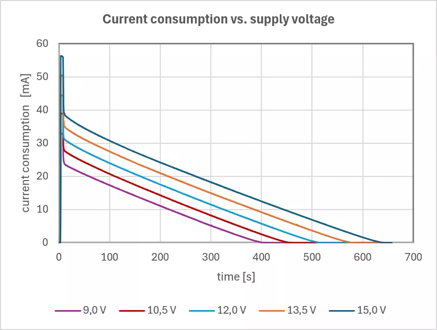
Because of the operating principle described above, the circuit’s current consumption varies throughout the timing cycle. It is highest while switch K is closed. After the switch is opened, the current quickly falls to a lower value and then continues to decrease as C1 charges, eventually becoming essentially zero.
I also measured the current consumption as a function of time at the different supply voltages. The results are shown in the graph below.
While measuring the current consumption, I noticed that if switch K is closed only very briefly, capacitor C1 does not have enough time to discharge fully. In that case, the remaining delay is extended, but the timing cycle does not restart completely from the beginning. This behaviour is shown in the following graph, which again plots current consumption against time. The timer was restarted with switch K at the points indicated by the red arrows. The fourth and fifth restart attempts are the ones where the timer was not completely reset; the remaining delay was merely extended.
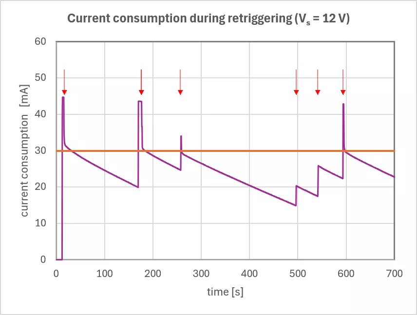
My digital multimeter can log data only at 0.5-second intervals, so during very short trigger pulses the rising edge of the current spike is not visible in the recorded data. I had promised my partner that we would go for a walk, so I did not set up the digital oscilloscope as well — that would have captured the current peaks in sufficient detail. Based on this measurement, with the component values used in my version of the circuit, switch K needs to remain closed for ⪆0.5 seconds to achieve a complete restart..
Flaws in the Circuit
At the beginning I mentioned the CMOS versions of the iconic NE555 timer IC. Their quiescent current is also very low, although still orders of magnitude higher than that of this extremely simple circuit. In terms of standby current, this little circuit therefore performs much better than the IC-based solution mentioned above. However, it also has several shortcomings, some of which may be significant in particular applications. One is the dependence of the timing interval on the supply voltage. Another is the uncertain restart behaviour when the trigger pulse is very short. Both have already been discussed, but there is also a third, minor design flaw: when K is held closed, electrolytic capacitor C1 is subjected to a small reverse-polarity voltage.
In the quiescent state there is no problem. T2 is off, so its collector is close to +Ut ≈ +12 V, while R1 holds the base of T1 close to 0 V. C1 is therefore charged to approximately the supply voltage with the correct polarity.
When K is closed, however, the base voltage of T1 rises to approximately UB_T1 = UBE_T1 + UBE_T2 ≈ 1.6 V. At the same time, T2 turns on and goes into saturation, so its collector voltage becomes approximately UC_T2 ≈ UCE(sat)_T2 ≈ 0.1 V. Note that the positive terminal of electrolytic capacitor C1 is connected to the collector of T2, while its negative terminal is connected to the base of T1. This means that when K is closed, the capacitor sees a reverse voltage of U_C1 = UB_T1 − UC_T2 ≈ 1.5 V.
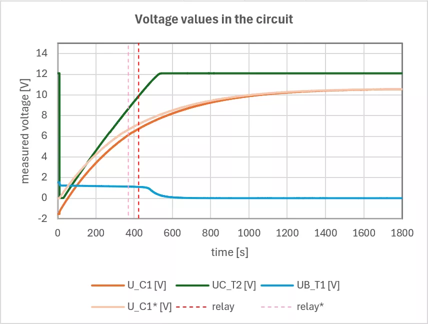
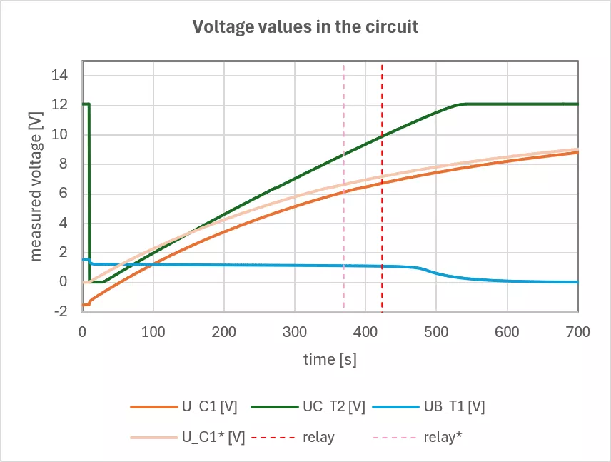
(the curves marked with * refer to a ‘cold start’; ‘relay’ indicates the switching point; U_C1 is the capacitor voltage, which, in the case of a ‘warm start’, has reversed polarity for approximately 50 ms after switch K is opened)
The original description says that when K is switched on, “capacitor C1 discharges”, but this is not entirely accurate. In reality, it first discharges and then charges to more than a volt in the opposite polarity. This also explains why the first timing cycle after power-up — when C1 really is discharged and has 0 V across it — is somewhat shorter than subsequent cycles initiated by pressing K. At first power-up, C1 charges from 0 V to +10,5 V, so the voltage change is ≈10,5 V. After K has been closed, however, it charges from approximately −1.5 V to +10,5 V, giving a total voltage change of ≈12.0 V.
Electrolytic capacitors do not tolerate reverse polarity. Manufacturers – such as Nichicon, the manufacturer of the capacitors I use – generally state that about 1 V is the maximum reverse voltage an aluminium electrolytic capacitor can withstand without damage. At higher reverse voltages, electrochemical oxide formation may begin on the cathode foil, gas may be generated, and prolonged or repeated exposure can reduce capacitance while increasing the dissipation factor and leakage current.
In this particular circuit, the reverse voltage is therefore borderline. According to manufacturers’ recommendations, an electrolytic capacitor should not be subjected to this much reverse voltage, although in practice many individual capacitors will tolerate it. I suspect that if the timer is used only occasionally and K is pressed only briefly, it will probably continue working for years without any obvious problem. Nevertheless, I would not call this good design practice, because if switch K is held closed continuously, C1 may eventually be damaged.
One correct solution is to replace C1 with a bipolar electrolytic capacitor. Such capacitors may cost two or three times as much as ordinary polarised electrolytics, but at these values the absolute cost is still negligible.
Another simple solution is to insert a silicon diode in series with T2’s collector, raising the collector voltage when T2 is on and thereby reducing the reverse voltage across C1 without interfering with T1’s base drive.
Afterword
While we were out walking, I told my partner about the results of the experiment. It is remarkable how much thinking, measuring and tinkering can come out of a circuit that I found entirely by accident and that, at first glance, looks almost ridiculously primitive.
And that is really the whole point. With apologies to Descartes:
“Mensuro, ergo sum.” — I measure, therefore I am.
My partner said that was all very well, but now that the timer was finished, what exactly were we going to use it for? I replied that figuring that out would be next weekend’s project. Maybe…